Laser Microprocessing
Introduction
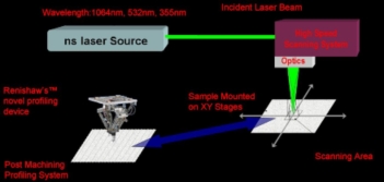
Effective laser machining of a variety of materials requires a number of different wavelengths and pulse lengths, requiring different types of high power lasers. We have a number of high power laser systems, of 3 main types: Nd:YAG, CO2, and Ti:Sapphire, which cover a wide range of wavelengths (355 nm to 10.6 ?m) and pulse lengths (100 fs to 20 ms; also cw) and hence can process a very wide range of materials, including metals, glasses, polymers and ceramics. There is a general trade-off between precision and process speed, with long (ms) pulses providing relatively coarse but high speed machining, whilst very high precision can be achieved by the much slower processes with ns or fs pulses. Often excellent microprocessing results are achieved using a combination of laser systems and/or pulse regimes.
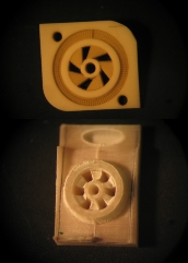
Micro-Engineering of Ceramics
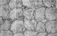
- Engineering ceramics are exceptionally difficult to machine using mechanical techniques
- Usually requires machining in a intermediate ‘unfired’ state
- This leads to dimensional change on firing making high tolerance micromachining impossible
- Lasers can be employed to machine material in final state
- ‘Clean’ machining of ceramics achievable by using nano-second lasers driven by a scanning system at reasonable process rates (~1 mm3/minute)
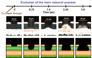
PCB’s Microvia Drilling
The context of this research project is the pivotal importance of interconnection and assembly technologies within the entire electronics industry, particularly those techniques based on circuit boards. These are driven by rapid market expansion, the imperative for increased process speed, quality and efficiency, and ever-shrinking semiconductor devices of increasing functionality which will demand higher component densities on circuit boards in the future.
This research is concerned with delivering competitive advantage in the form of:
- Commercially-viable process improvements for manufacturers of advanced electronics circuit boards
- Enhanced processes for integration in new machines for laser-based manufacturing system builders
- Data on new processes leading to laser specification requirements for laser manufacturers, coupled with early awareness of manufacturing technology directions.
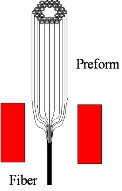
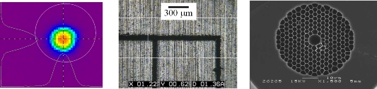
Fibre Delivery for Micromachining
- Micro-structured (photonic crystal) silica fibre with hollow (air) core
- Stacked silica capillaries form a macroscopic preform
- Preform is drawn down to final fibre dimensions
- Majority of power in air: can deliver much higher pulse energies in a single mode c.f. standard silica fibre
- First demonstration of micro-machining using output from a single, hollow-core photonic crystal fibre
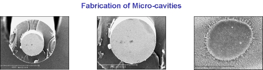
Fibre Optic Micromachining
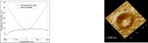
- Single pulse machined features on end facets of optical fibres for micro-etalons or micro-cavities.
- Sub-diffraction limited machining possible by altering focal position of the sample.
Microprocessing of Fused Silica
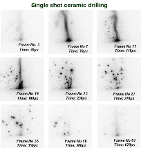
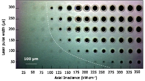
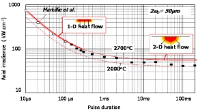
Ablation Process Characterisation
Shown below is detail of matrix from 50-300µs pulse duration for different values of irradiance
Short pulse duration:
=> Heat penetration depth << spot radius
=> Temperature controlled by energy
Long pulse duration:
=> Increased penetration depth, larger heated spot radius
=> Temperature controlled by power
Glass Micromachining Applications
- Fabrication of correction optics for laser diode arrays
- Fabrication of beam shape transformation optical elements
- Surface damage repair of optics
- Generation of Nano/Micro surface bumps
Other Applications
Development of micro-machining processes for a wide variety of applications
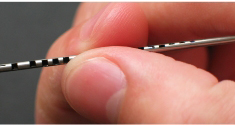
- In-vivo surgical instruments
- Surface treatment of aluminium as corrosion inhibitor
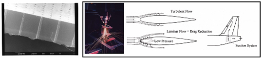
- Drilling holes in aircraft wings to reduce drag