
Facilities
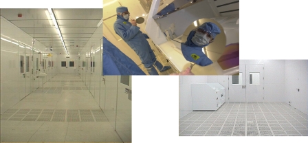
Full range of processing equipment for IC semiconductor and MEMS fabrication within a class 10 cleanroom environment
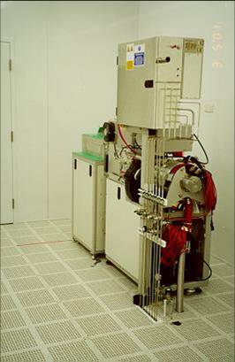
Inductively coupled plasma etcher for silicon deep etch (class 10 cleanroom)
Lithography - double sided aligner, projection stepper, e-beam (class 10 cleanroom)
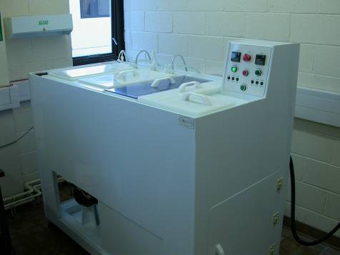
Electroplating: Two separate tanks for different electroplating solutions. DC and pulse-plating are possible. Suitable for wafer with a diameter up to 20 inches
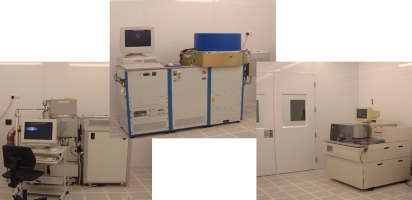
Plasma enhance vapour deposition, sputtering, CMP, wafer dicing, bonding, packaging (class 10 cleanroom)
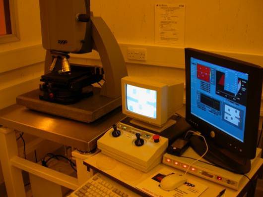
White light interferometer from Zygo with a resolution in vertical direction of 1 nanometer (class 1000 cleanroom)
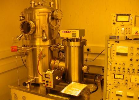
Physical vapour deposition - High vacuum electron beam evaporator suitable to deposit 4 different materials (class 1000 cleanroom)
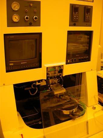
Karl Suss FC-6 Flip-Chip-Bonder (class 1000 cleanroom)
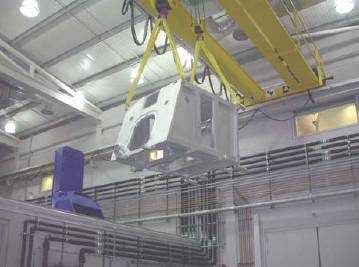
Optical assembly cleanrooms (class 100 – 10,0000), cryogenic test and flexure testing facilities (10 Tonnes max)
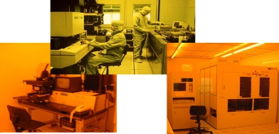
Chip repair, Analytical
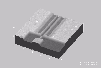
- Field Emission SEM (Philips XL40FEG)
- EDX analytical FESEM (Hitachi S4500II)
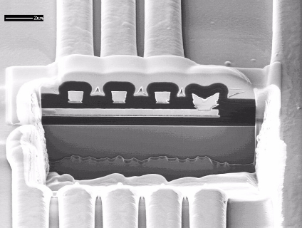
- FIB Workstation (FEI FIB200)
- AFM (Digital Instruments 5000)

NANO-INDENTATION (including nano-scratch, nanowear, and AFM)

Raman Spectrometry