MicroElectro-Mechanical Systems (MEMS)
Integrated Diagnostics for Environmental and Analytical Systems (IDEAS)
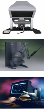
A small, robust, cheap and disposable multisensor microsystem that can transmit its measurement in real time is a valuable instrument to various applications, ranging from patient monitoring to industrial wastewater analysis. In the field of medical diagnostics, a capsule capable of traversing the gastrointestinal (GI) track taking advantage of the natural peristaltic motion of the gut could provide access to the small intestine that is currently unreachable by the traditional medical endoscopies.
The IDEAS project (with Glasgow and the ISLI) combined Lab-on-a-Chip (LOC) technology with the System-on-Chip (SoC) methodology to build an intelligent real-time measurement and monitoring tools.
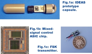
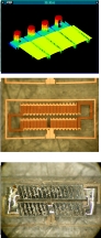
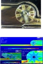
A multisensor microsystem prototype has been designed and implemented (Fig.1a). Four types of electrochemical sensors have been incorporated, namely pH, temperature, conductivity and dissolved oxygensensors. The sensor signal conditioning is provided by a mixed-signal control chip (Fig.1b). A power management scheme has also been implemented to ensure longevity of the power source. A FSK transmitter has been realised with discrete electronic components (Fig.1c). It operates at 38MHz and can transmit over a range of 1m.
The entire prototype weighs 13.5g and measures 16mm x 55mm. Using two SR44 Ag2O batteries, it can operate continuously for at least 76 hours.
Implantable Drug Delivery Microsystem
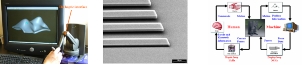
Most controlled drug release research has focused on degradable polymers and microfluidic devices. The former releases drug compounds continuously as opposed to the more effective pulsed pattern while the latter suffers from clogging or high viscosity solutions. Hence, a drug delivery device consisting of individually addressable micro-reservoirs which can release a small quantity of drug, on demand, becomes an attractive solution.
This project aims to integrate a drug delivery device, wireless power transfer system, a control chip and a pressure sensor into an implantable microsystem. We also aim to develop a drug release technique that will overcome the inevitable fibrosis efficiently, with low power consumption.
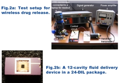
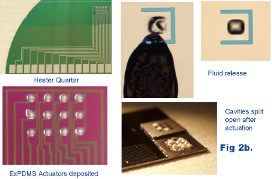
A 12-cavity drug delivery devices has been designed and fabricated (Fig.2b). They have been packaged into standard 24-DIL and custom packages for different in vitro and in vivo test purposes. The drug filling and sealing techniques have also been established. Additionally, we have built a RF powering system that operates at 7MHz and can provide sufficient energy to release drug remotely. Experiments show that the release rate is less than 10s typically, using 500Hz activation pulsestream.
Larger numbers of cavities will require integrated drive electronics and this will form the next stage of the project.

Active Electrowetting on Dielectric (EWOD) Device
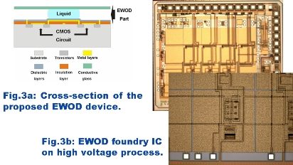
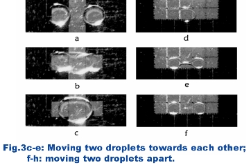
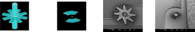
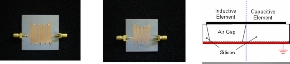
This project focuses on the issues associated with integrating electrowetting on dielectric (EWOD) technology (which moves droplets on electrode arrays) with IC foundry technology. The motivation is to increase the number of electrodes, allowing fine adjustment of the droplet size and the number of droplets. However, once the number of electrodes exceeds about 100, interconnect/packaging issues then dictate the use of an active CMOS backplane (Fig.3b).
A 100V CMOS process has been established to design a small array using transistors with high voltage shields (Si3N4 as passivation). An EWOD prototype device for 90V operation has been implemented. It is working as intended (Fig.3c-h).
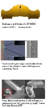
Sub-millimetre Common User Bolometer Array (SCUBA)
SCUBA-2 is a new generation wide field camera designed to replace SCUBA-1 and be operational on the James Clark Maxwell Telescope (JCMT) in Hawaii, USA in 2007.
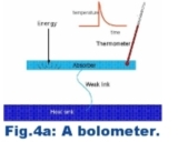
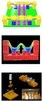
The new “CCD-like” array of detectors consisting of four 40 x 32 bolometer (pixel) arrays detects incoming radiation with wavelengths of 450 and 850mm and operates at 100mK. The bolometer consists of a sensitive thermometer and a high-cross section absorber connected by a weak thermal link to a heat sink.
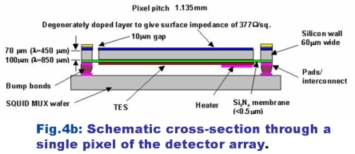
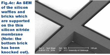
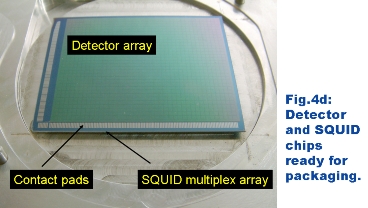
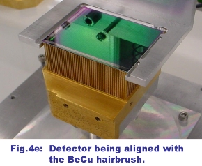
The chosen technology for the SCUBA-2 arrays is transition edge sensors (TES) read out by SQUID (superconducting quantum interference device) based multiplexers. A schematic cross-section through a pixel is presented in Fig.4b. The architecture is based on a hybrid design that consists of an upper detector chip and a lower multiplexer chip held together with indium bumps.
Fig.4d shows the detector indium bump bonded (with 218,000 bumps) to the SQUID Mux chip and Fig.4e illustrates the device being aligned to the BeCu hairbrush.
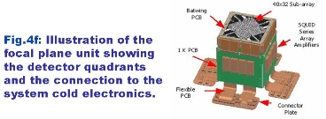
The assembled detector consists of four 40 x 32 sub-arrays and the focal plane unit is shown in Fig.4f.
High-Level Design
Chip/Wafer Bumping for Ultra-Fine Pitch Flip Chip Interconnections
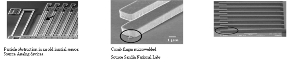
The aim of this project was to investigate a new chip/wafer bumping method for ultra-fine pitch flip chip interconnections. In this method bumps are fabricated on low cost, flexible carriers and then transferred onto chip/wafer for flip chip assembly. The new method minimises post-processing of IC wafers for bumping and offers ultra-fine pitch capability. Gold, copper and nickel micro-columns at sub-100 µm pitch were fabricated on polymer substrates. Electroless nickel and gold plating processes were developed to deposit nickel and gold layers on aluminium bond pads on IC chips. Bump transfer from carrier to silicon chip was successfully achieved with good bond strength between the bumps and IC chips.
Haptic technology for virtual interaction
The potential MEMS market is currently estimated at $11 billion and forecasted in 2007 over $26.4 billion, but surprisingly, there is a lack of modelling and simulation methodology for precise performance verification of MEMS products. So, the goal of this project is to design a digital tool using haptic computers, which will enable designers the facility to model and interact with their virtual prototypes in real time. Moreover, this technology will enable designers, the aptitude to analyse, refine, realise simulation of their prototypes for specific conditions such as internal/external environments or phenomena that can be arise in micro-, meso- or nano-scale without building any physical prototype until the later stage of the manufacturing process.
Failure modes and reliability models for MEMS
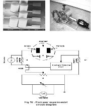
In the field of MEMS how the devices fail is not completely understood in many cases moreover reliability and yield models are still at research stage. Such immaturity in this field is perhaps one of the factors hindering the industrial take up and commercialisation of such devices as well as acceptance of this technology. In this project the different failure mechanisms in MEMS and their affect were studied. FMEA methodology has been applied to systematise the risk assessment of failure mechanisms in MEMS. Methodology for high level design of MEMS failure modes has been set up and is validated to model the environmental (pressure and temperature) influence on micromotor performance. The reliability models of various failure modes will be developed for specific MEMS.
MEMS Manufacturing
Manufacture and Characterisation of Microscale Magnetic Components
The need for faster switching, reduced losses and smaller components has driven switching frequencies of DC/DC converters into the range of 0.5MHz-10MHz. The limitation in going to higher switching frequencies lies in the loss of current magnetic components with frequency. Ferrites appeared to have reached their limits in terms of higher frequency operation at reasonable loss levels. Thin film magnetic alloys incorporated into microscale magnetic components are investigated as a potential solution to the increased power density required in power supplies of fast switching frequencies.
Optical fibre array manufacture
Researchers at Heriot-Watt University have developed a novel automated system for the insertion and active alignment of two-dimensional monomode and multimode optical fibre arrays using a scalable process. The research team is looking at developing a system which is suitable for mass production and also scalable to larger arrays of two-dimensional fibre bundles used in displays, e.g. up to 256 by 256. This will represent a significant enhancement in capability.
This technology will allow end users to produce highly accurate low-cost fibre arrays and remove one of the current bottlenecks in interconnection technology today.
Packaging of Micro-UV-LED/Lens-Array
This Basic Technology Programme project is a joint venture between Heriot Watt University, University of Strathclyde, Imperial College London and the University of Sheffield. The objective for the MISEC Team is the support of other partners in packaging issues in particular the assembly of a microlens array on top of a UV-LED array. The microlens array has to be placed highly accurate in lateral as well as vertical position. Furthermore it is anticipated that a vertical movement of the microlens array for adjusting the focal point will be implemented. The protection of the cavity between lenses and LEDs from chemical and physical influences is also an objective.
Microactuators
Practical and Simulation studies of Microturbines
Simulation studies have been carried out for a number of years using ANSYS to model microturbines. The possible levitation of the rotor in the cavity due to the pressure created over a step bearing has been investigated and simulation studies suggest that this could be a simple way to reduce friction in the turbine. Further detailed work is being undertaken and it is also being supported by practical studies to substantiate this effect Satisfactory development of these type of microturbines could lead to small power generation devices and air flow sensors
Electrical Breakdown at Micrometre Separations
For the expanding area of Microsystems and microactuators in particular, the electrical breakdown of materials at small separations becomes extremely important to understand. However measurements at these small separations are difficult to carry out and an apparatus was developed in house in order to allow this type of work to be undertaken. Measurements with different types of materials at increased pressure and reduced pressure can be carried out with the equipment
RF MEMS
Novel Microwave Filters for Implementation with MEMS
The aim of this project is to use MEMS technology to improve the performance and reduce the size of microwave filters. Without MEMS the dimensions needed to couple the resonators together has made size reduction difficult. Also techniques such as under etching the silicon below the conducting elements have allowed increase in performance as well as size reduction. Laminating the conducting lines has also increase the performance of the filters by reducing the conductor losses. All these processes would not have been possible without MEMS technology.
High Power RF/Microwave MEMS Switches
This proposed research aims to develop advanced RF/microwave MEMS switches that are capable of handling high power. MEMS switches have recently emerged as enabling devices for improving the cost-effect performance of microwave switching networks and systems. The near-zero power consumption, low intermodulation products, very high isolation and very low insertion loss are clearly properties that have attracted considerable research effort. In this Project new high power RF MEMS SPST and SPDT switches will be designed, fabricated and tested. The project will be collaborated with Rutherford Appleton Laboratory and BAE Systems Advanced Technology Centre.
Flip Chip Assembled MEMS Inductors for Wireless Communications
The aim of this project is to develop suspended MEMS inductors for wireless communications applications. Current IC process based micro-inductors suffer from low Q-factor due to substrate conductivity and will be a limiting factor in the performance of next generation RF integrated circuits. A new technique based on flip chip assembly has been developed for producing suspended MEMS inductor devices. Meander line and spiral inductors have been fabricated and assembled with an gap between the inductor structure and the substrate to reduce the parasitic losses. The devices have been characterised using coplanar probes and a microwave network analyser. Q-factor of ~ 20 after pad de-embedding has been obtained at ~ 2.5 GHz.
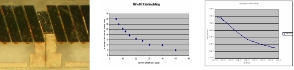
Magnetoelectric Composites for MEMS power generators
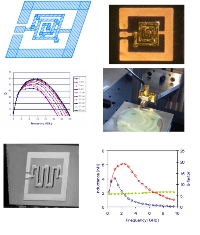
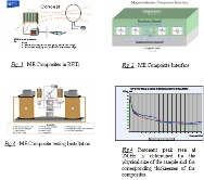
The aim of this project is to evaluate and model magnetoelectric materials for use as power generators for MEMS devices. The concept power generator is shown on Fig.1, for RFID applications. Stage 1 (current phase) is to evaluate the materials. ME composites can be configured in several ways, Fig.2. A variety of magnetostrictive and piezoelectric materials have been selected for their relevant properties piezoelectric and magnetostrictive coefficients. Samples have been tested, using the arrangement shown on Fig.3 and an output voltage vs frequency at 500G bias and 5G AC drive is seen Fig. 4. The ME composites were supplied by our collaborators, Cranfield University.
Cooling/Boiling system
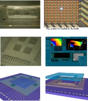
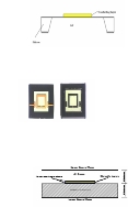
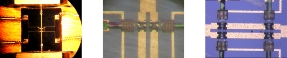
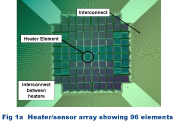
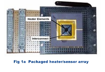
This system is a 96 element set of heater / temperature sensors with a resolution of ±0.1°C. Fig 1a shows the heaters and the interconnect. The heaters are tantalum and the interconnect aluminium.
Figure 1b shows the device in a package and it can be observed that the interconnect to the pads takes up considerably more real estate than the heaters. This graphically illustrates that about 100 elements is about the maximum practical number with hardwired connections. Arrays larger than 100 require an active backplane to address the elements.
The primary application for this device is to help characterise cooling systems using boiling.
Liquid Delivery
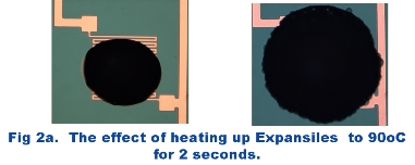
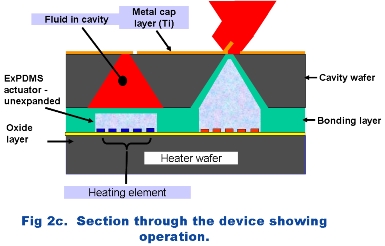
This approach to on shot liquid delivery is based upon Expansils which expand when heated. Fig 2a shows this effect with the right hand picture showing the effect of the Expansil being heated to 90oC for 2 seconds. Figure 2 shows the operation of the device with figure 3 showing a cross section.
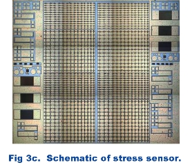
Stress Sensors
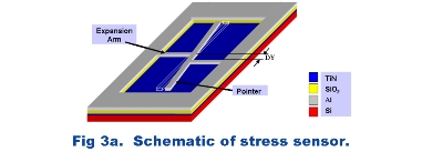
This sensor measures the stress in thin films. Figure 3a shows a schematic of the sensor with a clockwise rotation indicating compressive stress and anticlockwise a tensile stress.
This sensor measures the stress in thin films. The stress sensor is released by removing the SiO2.
Figure 3a shows a schematic of the sensor with a clockwise rotation indicating compressive stress and anti-clockwise a tensile stress.
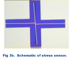
Figure 3b shows an example of the stress sensor showing compressive stress. Figure 3c show a test chip with a number of different designs.
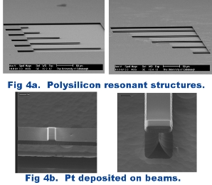
Resonant structures
The ability to actively adjust the resonant frequency of RF resonators has many attractions as it enables the resonator to be tuned to meet performance specifications and also to be fine tuned during its operation. Figure 4a shows polysilicon beams/bridges and figure 4b shows devices that have been tuned by depositing Pt on the beams using a FIB system. Similar operations have been performed on SiC beams of the same design.
The resonant frequency of beams has also been adjusted by moving silver along the beam in chalcoginide glass using current flow.
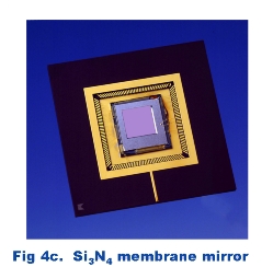
Deformable Mirror Membrane
Figure 4c shows a silicon nitride membrane mirror which is suitable for adaptive optics. The mirror is deformed using the array of electrodes located underneath it.
Polyimide membranes have also been implemented and exhibit lower driving voltages.
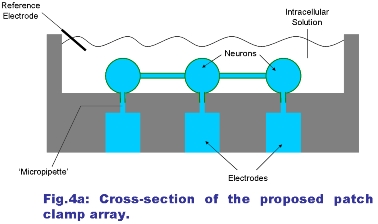
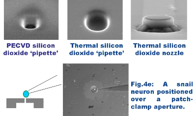
Planar Patch Clamp of Neurons on Silicon
This project aims to interface electronic systems to a living neural network using planar patch-clamp technology. Patch-clamp is an electrophysiological investigation technique, where by a glass electrode is used to rupture the membrane of a neuron, providing electrical access to the inside. By mimicking glass pipettes on a silicon substrate (planar-patch-clamp), the intention is to record and control intracellular voltages of many neurons simultaneously, and thus harness the computational function of the network.
At present, silicon devices with a pipette-like structure have been manufactured (see figures 4b-d), though no recordings have been made. Current work focusses on developing a system for aligning cell cultures to a planar device.
Electrodes
Electrodes are fabricated for a wide variety of uses which includes bio, electrochemistry, and electrostatic driving of membranes and liquids.
Microchannels
This technology has applications in microfluidics and lab on a chip.