
Mixed Signal VLSI Design and Neuromorphic Electronics
Introduction
The Institute of Integrated Micro and Nano Systems’ Mixed-Signal VLSI Design research covers a number of application areas:
- Sigma Delta Converters
- CMOS Image Sensors
- Biosensors
- Neural and Neuromorphic Computation
These fields can all interact and assist each other. In this particular case Neuromorphic VLSI is used to minimise the effects of transistor mismatch, a problem for all mixed signal design.

Neuromorphic Electronics
Neuromorphic Electronics are those which have been designed based on the architecture and design principles of the biological nervous system. Spike Timing Dependent Plasticity (STDP) belongs to a class of neural algorithms that operate on the individual inter-spike timings and not spike-rate correlations. STDP has been shown to have the ability to tune network performance.
As circuit geometries decrease, the problems associated with transistor mismatch increase. When sub-micron devices are operated sub-threshold the effect is exacerbated. Could a STDP technique correct for mismatch within neuromorphic circuitry?
The Context of this work is a spike timing driven algorithm for visual scene analysis which reduces the effect of noise by predicting the spike arrival time.
Design Requirements:
- Predict the arrival time of a spike from the timing of two previous spikes
- Evaluate the effect that process mismatch will have on the temporal characteristics using Monte Carlo Simulation
- Design an STDP adaptive network to compensate for the mismatch error
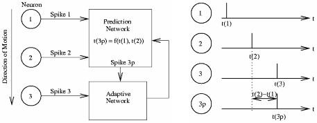
Neurons 1 to 3 fire at predetermined intervals. Neuron 3p fires at a time predicted from the firing time of neurons 1 and 2. If the neurons fire at equal intervals t(3p) = t(2) + {t(2) - t(1)} where t(1) is the firing time of spike 1, t(2) for spike 2 etc. Spike 3p is the prediction of spike 3. A previously fabricated circuit showed that the neurons can be activated by transient-detecting pixels, providing the necessary visual input.
Prediction, Mismatch and Adaptation
The prediction is made by charging a capacitor during the time between t(1) and t(2) and then discharging it with a matched current. The time at which the voltage across the capacitor reaches the starting point is when spike 3p fires. The prediction will be good if Vslope equals Vb and the transistors are well matched.
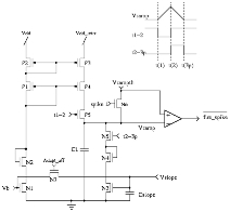
If the transistors are not well matched Vslope can be adjusted using the circuitry below:
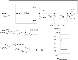
If spike 3 arrives before the prediction, Vslope must be increased. If the prediction arrives first, Vslope is decreased. The HiLo block provides two voltages, the high and low signals are approximately 200mv above and below Vslope respectively. These voltages are applied to Vslope using a switched capacitor technique. The amount of charge switched is dependent on the signals CS1-3 which turn on over time. In this way the change in Vslope is related to the time difference between spike 3 and spike 3p.
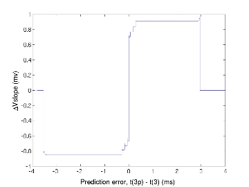
The change in Vslope against prediction error is plotted below:
Chip Layout and Test Results
Three blocks of the adaptive circuitry were laid out using a 0.35µm process. The layout was extracted and simulated using Monte Carlo methods to determine its ability to compensate for mismatch.
One hundred simulations were run and the prediction error, before and after adaptation, was measured. The results are shown below.

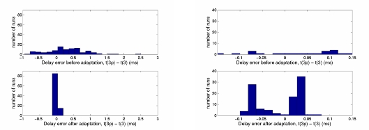
The results show a marked improvement on the original spread. When the x-axis is zoomed in, the effect of the adaptation algorithm can be seen. At a prediction error of zero the algorithm makes an abrupt change between ±6.5mV. This results in the post-adaptation error being made up of two groups a few milliseconds above and below zero.
The layout is being fabricated to verify these results.