
The Application of a Micromachined Three-Axis Accelerometer in Heart Bypass Surgery
Lars Hoff1, Craig Lowrie2, Marc P.Y. Desmulliez2, Ole Jakob Elle3 and Erik Fosse3
1Faculty of Science and Engineering, Vestfold University College, Horten, Norway
2Microsystems Engineering Centre (MISEC), Heriot-Watt University, Edinburgh, Scotland
3The Interventional Centre, Rikshospitalet University Hospital, Oslo, Norway
Abstract
This paper presents an overview of the design, manufacturing of a miniaturized heart sensor. The sensor is a micromachined three-axis accelerometer implantable inside the body of a patient. The sensor has for function to detect the risk of regional cardiac ischemia for patients who have just undergone coronary artery bypass surgery. The feasibility of this application has been proven in animal studies using commercially available sensors. This paper introduces the design requirements of a dedicated sensor and the processes required for the fabrication and packaging of such a sensor.
Introduction
Coronary heart disease (CHD) is caused by the narrowing of the small vessels that supply blood and oxygen to the heart. This narrowing stems from the build-up of fatty substances in the coronary arteries. Coronary heart disease is the UK's biggest killer, with one in every four men and one in every six women dying from the disease. In the UK, approximately 300,000 people have a heart attack each year [1]. One of the most common surgeries that is used to treat CHD is coronary bypass surgery. Coronary bypass surgery, medically known as coronary artery bypass graft or CABG, is an operation in which a blood vessel from another part of the body is grafted between the aorta (the main artery leading from the heart) and the coronary artery, or arteries, to bypass blockages and restore blood flow to the heart muscle.
Cardiovascular surgeons have extensive training in bypass techniques and CABG is one of the most frequently performed major surgeries in the world. However, a small percentage of these procedures suffer complications such as the re-occlusion of the bypass. The sensor is to be used by the medical staff in post-surgery to provide “real-time” monitoring of the heart and give early warning of regional cardiac ischemia. [2]
The sensors that are used in our studies are biocompatibally packaged so that the sensor is safe to bew implanted in the human body. This packaging of the accelerometer was carried out using a silicone moulding technique [3]. In order to operate on his heart, the thorax of the patient is opened prior to the bypass surgery. Following the bypass procedure, the sensor is stitched to the surface of the heart before closing the thorax. A cable, that carries the sensor input and outputs, is left protruding through a small hole in the patient’s chest. After a few days, once the medical staff have determined that the procedure has been a success and the patient is fit to leave the hospital, the cable is used to pull the sensor free from its stitches and out through the hole in the chest.
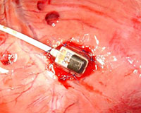
Figure 1 - Heart sensor stitched
to a heart during animal studies
The animal studies carried out to date have utilized the commercially available three-axis accelerometer from Kionix (KXM52-1050, Ithaca, NY, USA). One such sensor can be seen in-situ in Figure 1. The studies have proved that this type of sensor is capable of measuring the heart function in great details and provide early recognition of ischemia [4].
There is a strong requirement for the sensors to be as small as possible so that they do not affect the natural motion of the heart and cause as little difficulty as possible when pulling the sensor free from the heart and out of the chest. The commercial sensor implemented during the animal studies was considered too large for human trials. The dedicated sensor measures approximately 3mm in width, 5mm in length, and 1.5mm in height.
Accelerometer Structure
The various sensors fabricated have all the same configuration consisting of a basic seismic mass and cantilever beams. Four monolithic designs were submitted, each of which consisted of four full wafer thickness masses, each supported by either a single or two thin stress-sensitive beams.
To realise the seismic masses, Silicon-On-Insulator (SOI) wafers were processed using a deep dry etch process step This process allows the full wafer thickness to be etched for the definition of the silicon handle layer (380 µm thick). It also permits the definition of near vertical sidewalls. The buried oxide (BOX) layer represents the etch-stop from the backside due to etch selectivity. Finally, the silicon device layer can be used for the cantilever beams and these were chosen to be 4 µm thick. The schematic of one of the sensors is shown in Figure 2 (note that this does not include the bonding and bond pad areas).
The use of a deep dry etch versus an anisotropic wet etch has particular benefits for this sensor design. The etch rate is no longer dependent on crystal planes, which would result otherwise in angled sidewalls. Larger masses can therefore be fitted into a given footprint which increases the sensitivity of the sensor. In addition, the position of the centre of gravity of the masses in the vertical direction lies deep inside the wafer, which further increases the sensitivity to in-plane accelerations. There is also no requirement for compensation structures that are required in anisotropic etching to protect faster etching convex corners.
The critical dimensions of the sensor structures were defined such that a process limited maximum stress of 500MPa for 500g (acceleration due to gravity) of acceleration in any direction would not be exceeded. Tuning the dimensions of the structure to this value permits the maximum mechanical sensitivity possible to be attained. Other factors that determine the dimensions of the sensors include the overall size of the chip as suggested by the medical team for the application, the design rules regarding the sensing piezoresistors and the associated electrical connections for the piezoresistor bridges. The resulting chip dimensions for each of the designs are outlined in Table 1.
Table 1 - Dimensions of the fabricated designs (in µm)
| Design I | Design II | Design III | Design IV | |
| Chip Length | 3250 | 3250 | 3250 | 3250 |
| Chip Width | 2500 | 2500 | 2500 | 2500 |
| Mass Length, LM | 400 | 400 | 265 | 225 |
| Mass Width, WM | 800 | 800 | 700 | 552 |
| Thickness, TM | 384.5 | 384.5 | 384.5 | 384.5 |
| Beam Length, LB | 192 | 192 | 192 | 192 |
| Beam Width, WB | 60 | Varies | 60 | 80 |
| Beam Thickness, TB | 4 | 4 | 4 | 4 |
Working Principle
The four masses are designed to represent two pairs of masses. They essentially form two dual-axis accelerometers positioned at right angles to each other [5]. Both pairs of masses can measure out-of-plane acceleration. Taken individually, the can also measure in-plane accelerations. The behaviour of the masses under in-plane and out-of-plane accelerations can be seen in Figure 2 .
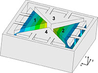
(a) |
(b) |
Figure 2 - Deformation of sensor masses when (a) in-plane (x-axis) and (b) out-of-plane (z-axis) accelerations are applied
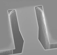
Figure 3 - SEM image of tapered
beam in Design II
The transduction and sensing of the acceleration is made possible using a network of piezoresistors. The piezoresistors convert the stress resulting from the mechanical deformation into a change in resistance. Sixteen piezoresistors, with different orientations, are implanted into the surface of the stress-sensitive beams. A piezoresistor to measure in-plane acceleration and another piezoresistor to measure out-of-plane acceleration are placed on each beam and are connected with the other piezoresistors to form four Wheatstone Bridges. These bridges are used to detect the changes in magnitude and direction of the acceleration.
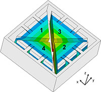
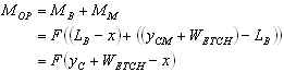
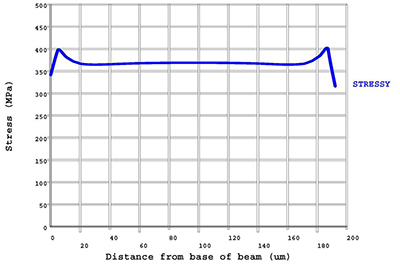
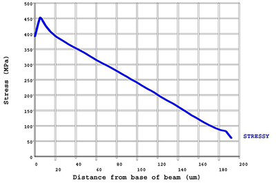
A cantilever beam with a rectangular profile has maximum stress at the base of the beam for out-of-plane accelerations. This stress decreases linearly along the length of the beam, making the placement of the sensing piezoresistors critical to achieve maximum sensitivity. Variations in the etch process step make the location of the base less accurate, which further complicates the placement of the resistor. Tapered beams, shown in Figure 3, alleviate this problem. Whereas, as in Figures 4(a) and 4(b), the stress decreases along the length of the beam, the simulated resulting stress profile in a tapered beam is nearly constant and of high magnitude, as shown in Figure 5, which allows the indiscriminate placement of the piezoresistors for maximum sensitivity.
Design and Simulation
Analytical calculations based on the theory of classical elasticity [6] and finite element analysis (FEA) using the commercial software package ANSYS, have been carried out for the design of these sensors. The motivation for this simulation is quantify the output performance of the structures as well as to provide a means for design optimization.
The major part of the design process was to verify that the maximum value of stress that the structures experience as a result of 500g of acceleration from any direction did not exceed 500MPa. The stress resulting from out-of-plane acceleration (σOP) is determined by the distance from the base of the beam (the fixed end) to the lateral centre of gravity of the mass:
| (1) |
where I is the moment of inertia of the rectangular cross-section of the beam, zCB (TB/2) is the vertical centre-of-gravity for the beam and MOP is the total bending moment, which is equal to the sum of the bending moment at the end of the beam and the bending moment for the mass:
 |
(2) |
In the above expression, F is the force exerted on the structure; x is the distance from the base of the beam; yCM is the lateral centre-of-gravity of the mass. WETCH is the width of the etched trench that releases the structure and is therefore the distance from the base of the beam (the support) to the start of the mass.
The centre of gravity of the mass (zCM) determines the in-plane stress (σIP):
| (3) |
where MIP is the bending moment for the in-plane stress:
| (4) |
The geometry of the masses has been designed such that it is theoretically possible to have matching sensitivities to in-plane and out-of-plane accelerations. To achieve this, it was required that the distance between the centre of the out-of-plane sensing piezoresistors and the lateral centre-of-gravity of the masses (yCM) is equal to the vertical centre-of-gravity for the mass (zCM = HM/2 = 192µm). To achieve this, the masses were wrapped around the supporting beams to bring yCM closer to the base of the beams.
(a)
(b)
Figure 4 - Stress distribution along length of rectangular beam for (a) in-plane and (b) out-of-plane accelerations
The stress distributions from FEA modeling along the length of the rectangular beams in Design I can be seen in Figures 4(a) and 4(b) for in-plane and out-of-plane accelerations, respectively. The distance from the base of the beam to the centre of the out-of-plane sensing piezoresistor is 30µm. At that point, the stress is 373 MPa as shown in figure 4(b). This compares to the constant stress distribution value in Figure 4(a) of 369 MPa. The values obtained analytically were 377 MPa and 372 MPa, respectively.
The simulated stress profile, caused by out-of-plane acceleration, in the first tapered region, nearest to the base of the beam, can be seen in Figure 5. When considering the respective stress distribution for a rectangular beam profile in Figure 4(a), the tapered region makes placement of the out-of-plane sensing piezoresistor non-critical.
Figure 5 - Stress distribution along length of tapered beam for out-of-plane acceleration
Fabrication
The accelerometers discussed here have been fabricated using a bulk micromachining process at the Scottish Microelectronics Centre, Edinburgh, Scotland. Some images of each of the fabricated sensors can be seen in Figure 6. The main process steps are discussed below:
- The wafer is a double side polished, n-type, (100) oriented silicon-on-insulator (SOI) wafer. The wafer consists of a 4µm thick silicon device layer, 0.5µm thick buried oxide (BOX) layer and a 380µm thick silicon handle layer.
- Thin oxide is grown on the front-side of the wafer using plasma-enhanced chemical vapour deposition (PECVD).
A photolithography step followed by a boron implantation defines the p-type surface conductors in the n-type silicon. This implantation is carried out where electrical connection is required between the piezoresistors and the bondpads.Another photolithography step is carried out and the second boron implantation is performed to define the p-type surface piezoresistors. These are placed on the stress-sensitive thin beams.The thin oxide is then selectively etched in areas above the implanted surface conductors. This is to provide an electrical connection between the surface conductors and the following metallization step.
- Aluminium is then sputtered on the front-side of the wafer. Photolithography is then followed by etching to form the metal conductors.
- Etching is then performed from the front-side of the wafer first. A reactive ion etch (RIE) is used to define the outline of the masses and the beams by etching through the silicon device layer. The BOX layer is used as an etch stop.
- The final lithography step is then done on the back-side of the wafer. The etch process uses an inductively coupled plasma (ICP) etch and is used to define the masses and the supports for the base of the beams. The 380µm thick silicon handle layer is etched first using the BOX layer as an etch stop. Finally, the BOX layer is then etched itself and this releases the structures, leaving the masses supported only by the beams.
|
(a) |
(b) |
|
(c) |
(d) |
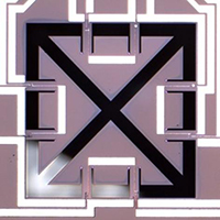

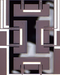
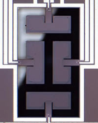
Figure 6 - Microscope images of the front-side of (a) Design I, (b) Design II, (c) Design III, and (d) Design IV
Packaging
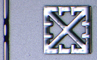
Figure 7 - Microscope image of
the back-side of Design II
The decision was made to perform the packaging at the chip level. To do this, it was necessary to remove each chip from wafer-level following completion of fabrication. Conventional dicing was not considered as a viable approach due to the high risk of damage from vibration and debris to the fully released sensitive structures. To overcome this issue, tabs were incorporated around the sensors and held the chips in place once processing was complete. An example of these tabs is shown on the left-hand side of Figure 7. A small amount of downward pressure “snaps” the chip free from the wafer.
To protect the sensitive structures of the sensor for handling and further biocompatible packaging, glass caps have been bonded to the front and back of the die. This was performed using a polymer based, low-temperature bonding process. Benzocyclobutane (BCB) is deposited and patterned onto the glass wafers [7]. No cavities have been etched into the glass caps so the thickness of the deposited BCB forms the gap for the movement of the masses under acceleration. The three components have been aligned under a microscope and pressed together by a weight. A heating cycle is then ramped up and down with the whole temperature-loading cycle taking approximately 30 minutes. A packaged sensor is shown in Figure 8.
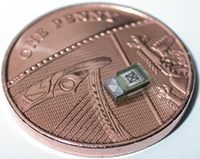
Figure 8 - Packaged sensor placed
on top of a one pence piece
To achieve a larger gap between the glass caps and the top and bottom of the masses, the possibility of using sandblasted glass spacer layers was investigated. The gap can be determined by the thickness of the glass used and puts less pressure on processing thicker BCB. BCB was also used to bond these layers in a glass-glass-silicon-glass-glass structure and was proven to be a viable approach.
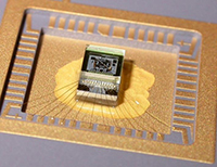
Figure 9 - Packaged sensor glued
and wirebonded in ceramic chip carrier
With the commercial sensor solution used during the animal studies, almost one third of the volume was occupied by the cable termination. An approach has been investigated involving using a ribbon cable instead of a round multi-wired cable. Two techniques that have been considered for bonding the ribbon cable to the sensor are wedge bonding and non-conductive adhesive bonding. [8] Two sets of bondpads have been used in the design layouts, smaller pads for using with the methods described above and larger bondpads to be used with traditional wirebonding for the purpose of characterization. An example of a wirebonded sensor can be seen in Figure 9. These would not be required in a further process run and would further reduce the size of the sensors. In addition, all the designs were made to be the same size in the wafer layout in case the tabs were not successful and a different approach had to be used. The tabs were a success so further miniaturization would be possible in a further run.
Conclusions
Four accelerometer designs have been designed and fabricated to be used as a sensor solution for measuring the heart wall motion of patients who have just undergone coronary artery bypass surgery. The feasibility of using a three-axis accelerometer in this application has been proven using a commercially available sensor. Approaches for the packaging have been demonstrated that allow for further miniaturisation and biocompatibility.
The designs are theoretically capable of having matching in-plane and out-of-plane sensitivities by taking advantage of the benefits offered by using an inductively coupled plasma etch together with silicon-on-insulator wafers.
The packaged sensors have been glued into a ceramic chip carrier and wirebonded so that they are ready for characterization. It is hoped that the sensors will be dynamically characterized using a scanning laser-Doppler vibrometer. Piezoelectric actuators to provide excitation, makes it possible to integrate the use of a vacuum chamber with a vibrometer to measure the sensor in different environments. Another approach being investigated is to use acoustic excitation using an air-coupled ultrasonic transducer.
Acknowledgments
The authors would like to thank Scottish Enterprise, the Regional Development Agency for Scotland, through the grant entitled IMemsDesign for their financial support. The authors would also like to acknowledge the support from the Scottish Microelectronics Centre and the Edinburgh Research Partnership (ERP) funded by the Scottish Funding Council (SFC). Financial support is also acknowledged from the Norwegian Research Council.
Thanks also go to Dr. Changhai Wang, Mr. Kun Zhao and Mr. Yves Lacrotte from Heriot-Watt University for their assistance with the packaging of the sensor.
References
- "Coronary heart disease", available at: http://www.nhs.uk/conditions/Coronary-heart-disease/ (accessed 15 January 2009)
- Hoff, L. et al, “Measurements of heart motion using accelerometers,” Proc 26th IEEE Engineering in Medicine and Biology Society, San Francisco, CA, Sept. 2004, pp. 2049–2051.
- Imenes, K. et al, “Assembly and packaging of a three-axis micro accelerometer used for detection of heart infarction,” Springer Biomedical Devices, Vol. 9, No. 6 (2007), pp. 951–957.
- Put a reference here on the signal processing of the detection of ischemia using the 3d acceleremoter.
- Velten T. et al, “Dynamic behavior of a new two-axis accelerometer,” Solid State Sensors and Actuators, Chicago, IL, June 1997, pp. 1217–1220.
- Young, W. C. et al, Roark's Formulas for Stress and Strain, McGraw-Hill (New York, 1989).
- Wang, C.H. et al, “Chip scale studies of BCB based polymer bonding for MEMS packaging,” 58th Electronic Components and Technology Conference, ECTC 2008, Florida, USA, pp. 1869–1873.
- Imenes, K. et al, “Micro ribbon cable bonding for an Implantable Device,” 2nd Electronics Systemintegration Technology Conference, ESTC 2008, Greenwich, UK, pp. 265-269.